Take a large open model, say one with 405 billion parameters, and store it at 16 bits per weight. That is 810 GB. The biggest GPU memory on the market as I write this is 288 GB. Store the model at 8 bits per weight instead and its weights still take 405 GB. There is no GPU it fits on, and there is not going to be one, because models have grown faster than memory for a decade and show no sign of stopping.
So the model is cut up, and fortunately it has a natural grain to cut along. A transformer, as LLM Basics showed, is a stack of near-identical layers, 126 of them in the 405-billion-parameter model, and a token passes through them one after another, each layer taking the previous layer's output as its input. Each layer is a few large matrices, about 3 billion parameters' worth in this model, or 6 GB at 16 bits. That structure gives two ways to divide the model between GPUs. Cut across the stack, and some layers go on this GPU, some on that one, with each layer's output handed to the next GPU. Cut along it, and each layer's matrices are sliced so that every GPU holds a strip of every weight and computes a strip of every result. Either way, generating a single token now requires the GPUs to exchange partial results, over and over, hundreds of times per token.
How independent are the layers? Not at all, along the stack. Layer 9 cannot start until layer 8 has finished, because its input is layer 8's entire output, so for a single token the stack is a strict chain and cutting across it buys no speed by itself: GPU 1 sits idle while GPU 0 works through its four layers, then GPU 0 sits idle while GPU 1 takes over. What rescues the cut is that different tokens are independent. Serving many users at once, or training on a batch, the GPUs form a pipeline, GPU 0 starting on the next token's first layers while GPU 1 is still working on the previous token's middle ones, and the idle gaps, which the field calls bubbles, shrink as more work is in flight. Within a layer the picture is the opposite. The rows of a matrix are independent of each other, which is why a layer can be sliced into strips that run at the same moment on different GPUs, and that cut does speed up a single token. The price is that the strips only ever hold partial results, and before the next layer can begin they have to be added together and handed to every GPU, twice per layer in a typical transformer.
That collation is the downside of splitting at all, and it is worth being clear who does it, because no piece of hardware does it on its own. The decision of where to cut is made by software before anything runs, by the framework serving or training the model. The exchanges themselves are done by a library called NCCL, one more storey of the software stack from Part 12, which provides the collective operations, an all-reduce that sums every GPU's partial results and gives every GPU the total, an all-gather that concatenates them, and plain sends and receives for the pipeline boundaries. These run as kernels on the GPUs themselves, moving data over NVLink or the network, and they are also where the GPUs synchronise: a GPU that reaches an all-reduce waits there until every other GPU has contributed, so the slowest GPU sets the pace for all of them. The CPU's part is the one it always has, queuing those kernels along with the arithmetic ones. The cost is real. An all-reduce across eight GPUs takes tens of microseconds even over NVLink, a model with 126 layers does it a couple of hundred times per token, and that overhead is a good fraction of the time a token takes, which is why the rest of this part is about making the links between GPUs as fast as they can possibly be. And that changes the question of this series. Up to now it has been "how does a GPU compute". From here it becomes "how do many GPUs behave as one", and the answer is a ladder of interconnects that makes the memory hierarchy of Part 10 look short.
PCIe is not enough
Part 12 ended with the road between host and device: PCIe, 64 GB/s each way on a Gen 5 slot. Suppose a model has been cut across two GPUs in one machine, and a kernel on GPU 1 needs the partial results that GPU 0 has just produced. It is the program on the GPUs that wants the data, not the CPU, but without a dedicated link the only road is PCIe: the bytes leave GPU 0, travel up to the CPU's PCIe controller, and come back down to GPU 1, and 64 GB/s is the ceiling. Against HBM's 3 to 8 TB/s, that is fifty to a hundred times too slow. A layer's activations for a large batch can be hundreds of megabytes, and sending them over PCIe takes milliseconds while the matrix multiply that produced them took microseconds. Tensor cores would spend their lives waiting on the bus.
The fix is a dedicated link between GPUs that never touches PCIe or the CPU. Nvidia's is NVLink, introduced with Pascal in 2016, and its growth is the cleanest illustration of how much the industry has bet on multi-GPU work:
| NVLink generation | GPU | Year | Bandwidth per GPU |
|---|---|---|---|
| 1 | P100 (Pascal) | 2016 | 160 GB/s |
| 2 | V100 (Volta) | 2017 | 300 GB/s |
| 3 | A100 (Ampere) | 2020 | 600 GB/s |
| 4 | H100 (Hopper) | 2022 | 900 GB/s |
| 5 | B200 (Blackwell) | 2024 | 1.8 TB/s |
| 6 | Rubin | 2026 | 3.6 TB/s |
Those are totals across all of a GPU's links, counting both directions, which is how Nvidia quotes them. Counted the same way, an H100's PCIe slot manages 128 GB/s, so NVLink is seven times wider. It is still a quarter of the HBM bandwidth, which is the right way to think about NVLink: fast enough that a well-designed program can overlap the talking with the computing, not fast enough to be ignored.
Side note: no NVLink on the cards you can buy. None of this is available on a consumer card any more. The last GeForce with an NVLink connector was the RTX 3090 of 2020, and its 3090 Ti sibling, whose bridge carried 112.5 GB/s between a pair of cards, and the last workstation card was the Ampere RTX A6000. Ada dropped it from the RTX 40 series and the RTX 6000 Ada alike, Blackwell kept it dropped, and the RTX PRO 6000 of Part 9's table has no link to a second card at all. Jensen Huang gave the reason at the RTX 40 launch: the I/O area on the die was wanted "to cram in as much AI processing as we could", and PCIe Gen 5 peer-to-peer would be "sufficiently fast" instead. On paper that is fair. A PCIe 5.0 x16 slot counted both ways is 128 GB/s, a shade more than the 3090's bridge.
In practice it is not quite the trade it sounds. The RTX 40 cards shipped with PCIe 4.0, half that, and the 50 series is the first with Gen 5. More to the point, Nvidia's driver does not enable peer-to-peer transfers between GeForce cards over PCIe, so two 4090s in one machine exchange data by way of host memory, which costs a copy each way and the CPU's attention. The honest reading is that a fast link between two cards is a data-centre feature now, sold with the data-centre parts at 900 GB/s and up, and a pair of gaming cards is fine for data parallelism, where they exchange gradients once per training step, and poor for tensor parallelism, where they would have to talk at every layer.
Who knows where the data is
A natural question is who does the finding. When a kernel on GPU 1 needs a number that lives in GPU 0's memory, does the CPU translate, does the GPU know, or does the program have to copy it first? The answer is that the hardware knows and the program decides.
CUDA gives every allocation in a program a unique address, whichever GPU it sits on, and once the driver has enabled peer access between two GPUs, it fills in each GPU's page tables so that the addresses of the other's memory are marked as living over the link. From then on a kernel on GPU 1 can simply read through a pointer to GPU 0's memory. The load leaves the SM like any other, carrying a virtual address, and GPU 1's memory management unit looks it up, first in the SM's small translation cache and then in the page tables: for a local address the entry gives a place in GPU 1's own HBM, and for a peer address it says that the page lives on GPU 0, across the link, the same way a CPU's page table can say a page lives on disk. The chip's internal crossbar, the fabric that normally delivers a load to an L2 slice and its memory controller, delivers this one instead to the NVLink controllers on the edge of the die, which send the request out. On the far side GPU 0's NVLink controller turns it into a location in GPU 0's HBM and hands it to GPU 0's own L2 and memory controllers, which serve it exactly as if one of GPU 0's SMs had asked, and the number comes back the same way, with no CPU involvement at all. The memory controller doing the work is GPU 0's, and GPU 1 keeps no copy of the data in its own L2, which is one reason a read across the link costs several times a local one. The same works for the copy engines: a copy from one device pointer to another runs over NVLink directly. The CPU's only part is what it always is, setting up the page tables once through the driver and queuing the kernels.
So the GPU knows where the data is, at the level of addresses, and the program does not have to. What the program does have to know is where the data is at the level of performance, because a read over NVLink costs several times a read from local HBM. That is why real programs do not scatter reads across the domain but copy what they need in bulk, or arrange the cut so that each GPU mostly reads its own memory and exchanges partial results in a few large collective operations. The CUDA code for those exchanges is the same whether the path underneath is NVLink or PCIe: the same peer copies and the same NCCL calls. What changes is the speed, and whether peer access is possible at all, since a PCIe topology that cannot forward traffic between two slots makes the driver fall back to staging through host memory. NCCL discovers the topology when it starts and chooses its routes accordingly, so the program's author usually finds out which links they have by looking at the numbers rather than at the code.
Everyone talks to everyone
A link joins two GPUs. With eight GPUs in a server, connecting every pair directly needs seven links per GPU, 28 in all, and each pair then gets only a seventh of the GPU's bandwidth. Add more GPUs and the count grows with the square. Early multi-GPU boards compromised, with each GPU having fast links to some neighbours and slower paths to the rest, and programmers had to care which GPU held what. Nvidia's answer, from Volta onward, was the NVSwitch: a chip that does for NVLink what an Ethernet switch does for a network, so that every GPU can talk to every other at full NVLink speed at the same time. A board with eight GPUs and a set of NVSwitches is called an HGX, and Nvidia's own server built around one is the DGX. An eight-GPU HGX H100 node has 640 GB of HBM and every GPU in it can reach every other at 900 GB/s. For years, that eight-GPU box was the atom of AI infrastructure.
It is worth being precise about what the switch does, because the name invites a confusion. NVLink is the wire: a GPU's 18 ports and the lanes that run from them. NVSwitch is the junction those wires plug into, and you need both, just as an office needs both the Ethernet cables and the box they all run to. On an HGX H100 board there are four NVSwitch chips, each with 64 NVLink ports, and each GPU divides its 18 links among the four, so that no GPU is wired to any other GPU at all. Every link goes to a switch. Inside the switch is a crossbar, the same idea as the multiplexers of Part 5 scaled up: any input port can be connected to any output port, and all 64 can carry traffic at once without getting in each other's way. A request from GPU 1 for an address in GPU 6's memory goes out on one of GPU 1's links, the switch reads the destination and forwards it to one of GPU 6's links, and the answer comes back the same way, in a few hundred nanoseconds more than a direct wire would take. Because the switch does this for every pair simultaneously, each GPU gets its full 900 GB/s to whichever GPU it is talking to, or spread across all seven, and the whole board behaves as one NVLink domain in which any GPU can read any other's memory through a pointer, exactly as in the two-GPU picture above.
Where the switch physically lives answers a question people reasonably ask, which is whether it is a card. It is not. Data-centre GPUs in these systems do not come as PCIe cards at all but as SXM modules, flat boards that bolt face down onto a large baseboard, and the NVSwitch chips are soldered onto that same baseboard, with the NVLink lanes running as copper traces between the GPU sockets and the switches. The baseboard is the HGX. It then connects to the server's ordinary motherboard, where the CPUs live, over PCIe, usually through a set of PCIe switches, and that PCIe connection carries only what PCIe always carries here, the host's commands and copies. The NVSwitch has no place in it. The chips do have a small management connection, through which a service on the host called the fabric manager loads their routing tables when the machine boots, but no data ever reaches a switch except over NVLink. In the NVL72 rack the arrangement is the same idea at a larger scale: the GPUs sit in compute trays, the switch chips in their own switch trays, and both kinds of tray plug into a copper backplane at the back of the rack, about five thousand cables' worth, that Nvidia calls the NVLink spine. What you buy is therefore never a switch on its own. On the desk, two consumer or workstation cards can be joined by a short NVLink bridge with no switch at all, which was the RTX 3090 and A6000 arrangement, and that gives two GPUs a direct link and nothing more.
And here is what the real thing looks like, one generation on, with everything under its heatsinks.
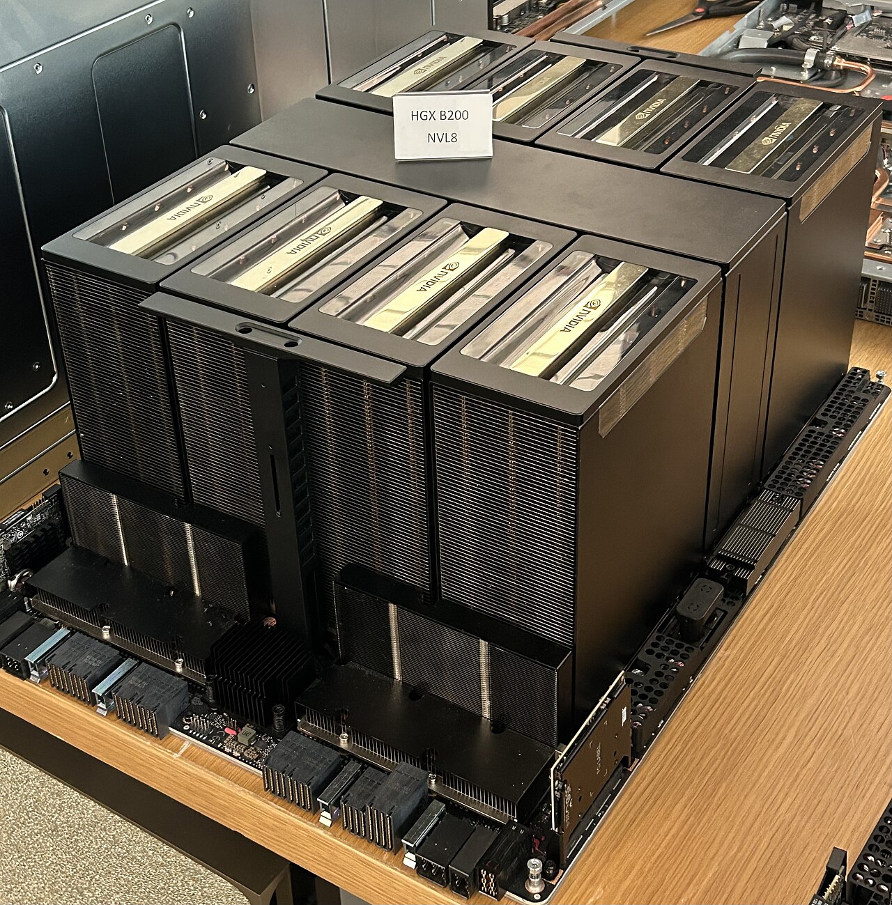
The newer switches do two more things. They know the topology, so that spreading a GPU's links across several switch chips gives it several independent paths and a broken link costs bandwidth rather than connectivity. And since Hopper they contain arithmetic of their own, for a protocol Nvidia calls SHARP: when eight GPUs all-reduce their partial results, instead of every GPU sending its numbers to every other and adding them up, the GPUs send their numbers to the switch once, the switch adds them as they pass through, and it sends the totals back to everyone. That roughly halves the traffic for the most common collective in the whole business, and it means part of every all-reduce in a Blackwell rack is computed in the switch rather than on a GPU.
Blackwell moved the boundary. The GB200 NVL72 is a full rack, 72 Blackwell GPUs and 36 Grace CPUs across 18 compute trays, with 9 trays of NVSwitch chips wired so that all 72 GPUs form one NVLink domain with 130 TB/s of total bandwidth between them. That is 13.4 TB of HBM in a single addressable pool. A model that needs 800 GB fits with room to spare, and to the software, the rack looks much like one enormous GPU, with the caveat that reaching a neighbour's memory over NVLink is still several times slower than reaching your own. The rack draws around 120 kW, roughly what a hundred homes use, and is cooled by liquid piped through every tray, because there is no way to move that much heat with air. Vera Rubin's rack keeps the same 72-GPU shape with everything doubled, and Part 18 has the numbers.
The ladder, now with rungs below the die
Beyond one rack, the next rung down is the ordinary datacentre network, InfiniBand or Ethernet, with a network interface card (NIC) per GPU running at 400 or 800 gigabits a second, which is 50 to 100 gigabytes. Another tenfold drop. Training a frontier model uses tens of thousands of GPUs, so most pairs of GPUs in such a system are connected through this bottom rung, and the art of distributed training is arranging the work so that the heavy traffic stays on the fast rungs.
How long does it take to move a given amount of data across each rung of the ladder? Pick something to move.
Each rung is several times slower than the one above it. The ladder from Part 10 had four rungs, registers, shared memory, L2, and HBM. This part adds four more below them: NVLink, the CPU link, the network, and PCIe. A number can live at any of eight levels, and the entire craft of running large models is keeping each number as high up the ladder as its use allows.
Three ways to cut a model
How the work is split across GPUs determines which rung carries the traffic, and there are three basic cuts, usually combined.
Data parallelism gives every GPU a complete copy of the model and a different slice of the data. During training, each GPU computes gradients on its slice and then all of them average their gradients before updating, an operation called an all-reduce that touches every weight in the model. It happens once per training step, which is rarely enough that it can go over the network. It also requires the whole model to fit on one GPU, which for large models it does not.
Tensor parallelism slices each matrix across several GPUs, so that each holds a strip of every weight and computes a strip of every result. The strips have to be combined at every layer, hundreds of times per token, so this cut needs the fastest rung available. It stays within an NVLink domain, which is the reason the domain exists and the reason it keeps growing.
Pipeline parallelism puts the first layers on one GPU, the next layers on another, and so on, passing activations from stage to stage. Only the layer boundaries need to communicate, so it tolerates slower links, and a large training run typically uses tensor parallelism inside each node or rack, pipeline parallelism across racks, and data parallelism across everything. The collective operations underneath all of this, the all-reduces and all-gathers, come from a library called NCCL, one more storey of the software stack from Part 12.
The superchip
There is one more link to name, and it changes the relationship from Part 12. A Grace CPU is Nvidia's own processor: 72 Arm cores with up to 480 GB of ordinary LPDDR5X memory. On a GH200 or GB200 board it is joined to the GPU not by PCIe but by NVLink-C2C (chip-to-chip), a 900 GB/s link that also makes the two memories coherent: the GPU can read the CPU's memory directly, as if it were a slower part of its own. Nvidia calls the pair a superchip. The point is capacity. HBM is fast and scarce, LPDDR5X is slow and plentiful, and with a coherent link a model can keep its most-used weights in HBM and let the rest, or the growing conversation cache of a long chat, spill into the CPU's half-terabyte at a speed only a few times below HBM rather than fifty. GB200 puts one Grace beside two Blackwells, and the NVL72's 36 Grace CPUs contribute 17 TB of LPDDR5X to the rack.
Where this leaves us
The unit of "a GPU" has been growing throughout this series: a lane, an SM of 128 lanes, a die of 144 SMs, then, from Blackwell on, a package of two dies, a node of eight packages, and now a rack of 72 in one NVLink domain, drawing 120 kW and cooled by liquid. Nvidia designs and sells the rack. It is, in every sense that matters to the software, one machine.
The growth was forced, not chosen. Models outgrew a die, then a package, then a node, and each time the interconnect had to become part of the computer rather than a cable between computers. Keep the ladder in mind. When Part 17 says NVLink 5 doubled to 1.8 TB/s, and Part 18 says NVLink 6 doubled again, you will know why those numbers get top billing next to the tensor core figures.
We have now assembled the whole machine from the switch up. The last six parts look at how it was actually built, generation by generation: first a short history of how Nvidia got from a graphics chip to the A100, and then one part each for Ada, Hopper, Blackwell, and Vera Rubin.
Next: A Short History: from the G80 that first let a graphics card run C, through Fermi, Kepler, Maxwell, Pascal, Volta, Turing, and Ampere, and the three eras those chips belong to.