Look at a photograph of the AD102 die, the chip inside an RTX 4090, and the first impression is of a city seen from the air. There is a grid of large identical blocks, twelve of them, each subdivided into a dozen smaller identical blocks, with a broad band of something else running down the middle. The big blocks are graphics processing clusters (GPCs). The small blocks inside them are streaming multiprocessors (SMs), and there are 144 on the full die. The band down the middle is the L2 cache, which is Part 10's business.
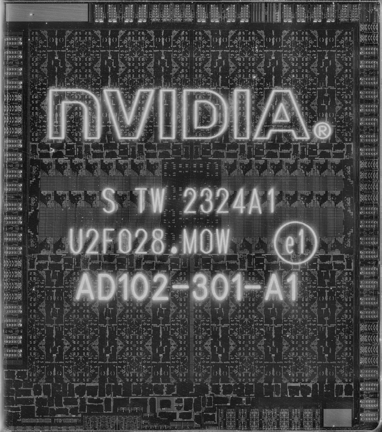
Here is the same photograph with the blocks labelled.
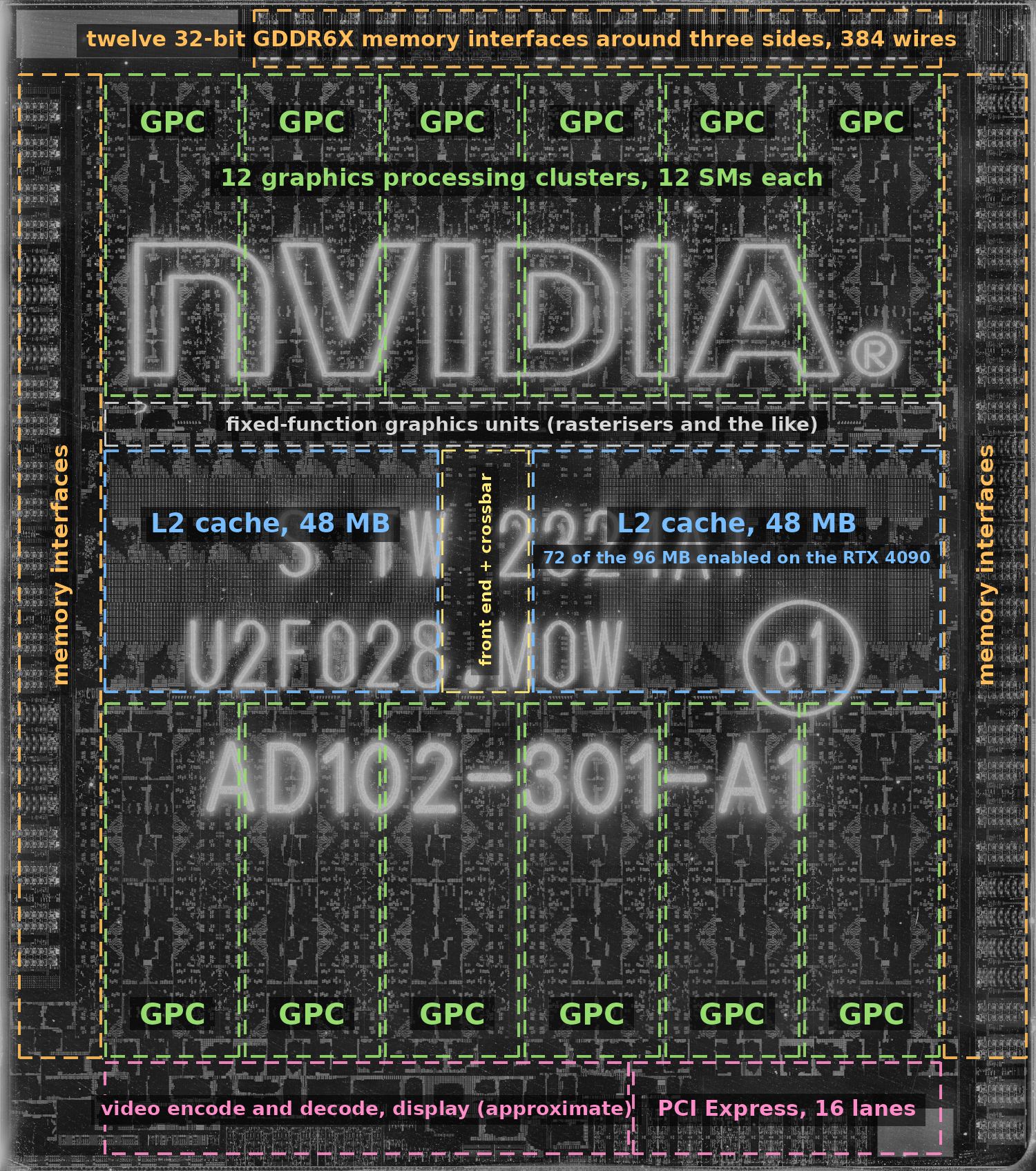
And here is the same chip the way Nvidia draws it in its own documents, as a block diagram of the full die. Every small cell is one SM, every pair of cells is one TPC, and the blocks that hold them are the GPCs. The photograph and the diagram are the same twelve blocks, the same cache band, the same ring of memory interfaces.
The SM is the unit that matters. When Nvidia says a GPU has 16,384 CUDA cores, what it means is 128 SMs with 128 lanes each. When it says a new generation is faster, most of the change is inside the SM. And when you want to understand why a GPU does well on one job and badly on another, the SM is where the answer lives. This part opens one up.
The floor plan
An SM on Ada or Hopper is split into four identical quarters, which Nvidia calls processing blocks or partitions. Each quarter has its own warp scheduler, its own bank of 32 lanes for ordinary floating-point and integer arithmetic (Ada makes 16 of them capable of integer work as well), its own quarter of the register file, one tensor core, and a few units for loading and storing data. Shared among the four quarters are a block of fast memory that serves as both L1 cache and programmer-controlled scratchpad (128 KB on Ada, 256 KB on Hopper), the special function units that compute things like sine, exponential, and reciprocal, and on a graphics chip an RT core for ray tracing.
Add up the four quarters and one SM has 128 lanes, four tensor cores, and 256 KB of registers. Multiply by 128 SMs and you have the RTX 4090's 16,384 CUDA cores and 32 MB of register file, which is more fast on-chip storage than most CPUs have cache. That was Part 7's point made concrete: the GPU spends its silicon on keeping thousands of threads' numbers on the desk, not on caches.
Warps, and the scheduler's tick
Now the part that makes it all work. A warp is a group of 32 threads that the hardware handles as one unit. Each thread in the warp is, from the programmer's point of view, its own little program with its own variables. From the hardware's point of view, a warp is one instruction stream, and when the scheduler issues an instruction, all 32 lanes carry it out at once, each on its own thread's registers. This is the one-front-end-feeding-32-lanes arrangement of Part 6, and the number 32 has been baked into every Nvidia GPU since the G80 in 2006.
It helps to be clear about what is hardware here and what is not. The 32 lanes in the drawing are hardware: thirty-two physical multiply-add units under one scheduler, and there are only ever those 32. A warp is not a piece of hardware. It is 32 threads' worth of state, their program counter, their registers, and a mask saying which of the 32 are active at the moment, and it is a unit of work rather than a unit of machinery. Nobody writes a warp, either. The programmer writes a program for one thread and asks for blocks of threads, and the hardware slices each block into warps of 32 consecutive threads by itself. So the thread and the block are ideas that belong to the software, the lane belongs to the hardware, and the warp is the seam where the two meet: a group of threads defined by the hardware because it maps onto the lanes one for one. The warp is invisible in the code and unmissable in the performance, because divergence, memory coalescing and the shuffle instructions all work per warp. What makes the seam matter most is that many warps share one set of lanes.
Each partition can hold many warps at the same time, not just one. On Ada an SM can keep 48 warps resident, twelve per partition, which is 1,536 threads. Hopper stretches that to 64 warps and 2,048 threads. Every resident warp has its registers permanently allocated in the register file, which is why the register file is so large. And on every tick, each scheduler does the same simple thing: look at its dozen resident warps, find one whose next instruction is ready to run, and issue it.
So what does a warp actually own? Very little, and that is the design. It owns its slot in the scheduler, its program counter and its active mask, and a slice of the register file: 32 threads times however many registers the program needs, which at full occupancy on Ada is about 42 each, so around 5 KB. Everything else in the partition is shared with the other resident warps and used by one warp per tick: the scheduler itself, the instruction cache, the 32 lanes, the tensor core, the special-function and load-store units. And everything outside the partition, the L1 cache and shared memory, the texture units, the RT core, is shared by all four partitions of the SM. One warp issues per tick per partition, but because the lanes are pipelined and the tensor core and the load units run on for many ticks once started, several warps usually have instructions in flight at the same moment.
That single sentence is the GPU's answer to the memory wall. Suppose warp 3 executes a load from memory, and the data will take 400 ticks to arrive. The scheduler does not wait. On the next tick it looks again, finds that warp 7 has a multiply ready, and issues that. Then warp 1, then warp 9, round and round. Warp 3's registers sit untouched in the file, so when its data finally arrives the scheduler can pick it straight back up. There is no context switch, no saving and restoring, no cost at all. As long as there is always some warp ready, the lanes never idle, and the 400-tick wait is invisible.
The fraction of an SM's warp slots that are actually filled is called occupancy, and it is the first thing a GPU programmer looks at when something runs slowly. Low occupancy means few warps to switch between, which means memory stalls start showing through. The usual cause is greed: if each thread uses a lot of registers, fewer threads fit in the file. At full occupancy on Ada, 65,536 registers shared among 1,536 threads leaves each thread about 42. A thread that wants 100 registers cuts the SM's occupancy by more than half.
Here is the classroom picture I use, since it holds up well. The SM is a classroom with four teachers. A warp is a row of 32 pupils. Each teacher reads out one instruction, "multiply the number on your sheet by the one next to it", and every pupil in the row does it to their own sheet. When a row has sent to the library for a book and is waiting, the teacher simply turns to another row. The place the analogy breaks is the important one: real pupils could get on with something else while they wait, whereas a lane cannot. Only the scheduler can switch, and only between whole rows.
When the row disagrees
Lockstep has a cost, and it shows up the moment the 32 threads of a warp reach an if and do not all agree. Suppose the instruction is "if your number is positive, do step A, otherwise do step B", and twenty of the threads have positive numbers. The hardware cannot send twenty pupils one way and twelve the other. There is one instruction stream. So it runs step A with the twelve non-positive lanes switched off, and then runs step B with the twenty positive lanes switched off. Both paths execute, one after the other, and the warp takes as long as A plus B. This is branch divergence, and it is the price of sharing one clerk across 32 calculators.
One warp reaches if (x > 0) { A } else { B }. Drag the slider to change how many of the 32 threads take the if branch, and watch which lanes work in each pass.
pass 1: run A (lanes not taking A are masked off)
pass 2: run B
Notice that the split does not matter. One dissenting thread costs as much as sixteen, because the whole of B has to run either way. Efficient GPU code is written so that the threads of a warp make the same decisions, or so that the decisions are made by whole warps at once. Graphics has always been like this, because neighbouring pixels usually do the same thing, and matrix arithmetic has no branches at all, which is one more reason a neural network suits the machine. Since Volta the hardware has been able to interleave the two paths rather than strictly finishing one before the other, which fixes some awkward cases, but the cost in lane-time is unchanged.
From SM to die
The rest of the die is organisation. Two SMs make a texture processing cluster (TPC), six TPCs make a GPC, twelve GPCs make an AD102. When a program launches work on the GPU, a unit called the GigaThread engine hands out blocks of threads to SMs that have room, and refills them as they finish. A GPU product is rarely the full die: the RTX 4090 has 128 of the 144 SMs enabled and the H100 has 132 of 144, because some SMs on each manufactured chip have defects, and disabling a few lets more chips be sold rather than thrown away.
The same drawing works for any Nvidia chip, and putting two others beside AD102 shows how much the recipe can vary while the SM stays the unit. First the H100's chip, GH100, drawn as in Figure 7 of Nvidia's Hopper whitepaper, and then GB202, the chip in the RTX 5090 and the RTX PRO 6000 Blackwell.
| AD102, RTX 4090 | GH100, H100 SXM5 | GB202, RTX PRO 6000 Blackwell | |
|---|---|---|---|
| Architecture, year | Ada Lovelace, 2022 | Hopper, 2022 | Blackwell, 2025 |
| Transistors, die area | 76.3 billion, 608 mm² | 80 billion, 814 mm² | 92.2 billion, 750 mm² |
| GPCs and SMs on the full die | 12 GPCs of 12 SMs, 144 | 8 GPCs of 18 SMs, 144 | 12 GPCs of 16 SMs, 192 |
| SMs enabled on the product | 128 | 132 | 188 |
| CUDA cores enabled | 16,384 | 16,896 | 24,064 |
| Tensor cores, RT cores | 512, 128 | 528, none | 752, 188 |
| L2 cache enabled | 72 MB | 50 MB | 128 MB |
| Memory | 24 GB GDDR6X, 384-bit | 80 GB HBM3, 5 stacks | 96 GB GDDR7, 512-bit |
| Memory bandwidth | 1,008 GB/s | 3,350 GB/s | 1,792 GB/s |
| Link to other GPUs | none | 18 NVLink links, 900 GB/s | none |
| Board power | 450 W | 700 W | 600 W |
Read across the three and the pattern of the series so far repeats at chip scale. The SM is the same kind of unit in all of them, and the differences are in how many there are, how they are grouped, and what feeds them. GH100 has fewer, larger GPCs and spends its edge on HBM and NVLink rather than on a wide ring of GDDR controllers, because its job is to keep 132 SMs fed with matrix arithmetic and to talk to seven other GPUs, and it drops the RT cores a graphics chip needs. GB202 is the same recipe as AD102 with everything turned up: a third more SMs, a third wider memory bus, and an L2 that is nearly twice the size, on a die a quarter larger. Part 15 through Part 17 go through each of these chips in turn.
Where this leaves us
A GPU is a few dozen to a couple of hundred copies of one building block, and that block is the SM: four schedulers, each issuing one instruction per tick to a warp of 32 lanes, choosing among a dozen resident warps so that the arithmetic never has to wait for memory. Everything Nvidia has done with the SM for a decade is variation on this theme, and the counts on a spec sheet, CUDA cores, tensor cores, threads per SM, register file size, are all just multiples of it.
What the SM cannot do on its own is keep itself fed. Each lane does a multiply-add every tick, and every one of those needs two numbers in and one out. Across a whole chip that is tens of trillions of numbers a second, and the memory of Part 7 delivers nowhere near that. How the gap gets closed is the next part, and it is where the design of a GPU becomes a design of its memory.
Next: Feeding the Cores: the GPU memory hierarchy from registers to HBM, the roofline that tells you whether your job is starved of arithmetic or of bytes, and why a language model generating text is almost always the second.